b) Add (at least) a button and LED (with current-limiting resistor)
c) Make it
The hello world board
I paid a visit to the fab academy website to get some idea on what is echo hello-world board. Echo Hello-World Board
As i do not have strong background on in any electrical and electronic, the more I read the more confused I become. If I diligently followed the guide in the fab academy schedule, I concluded I'll be able to finished all of them in 2017 or after. I decided to check out other people work on this week Electronic Design to have some "inspirations".
After some web searching I finally found something I can understand. Yadu Sharon's Echo Hello World Board Echo Hello-World Board
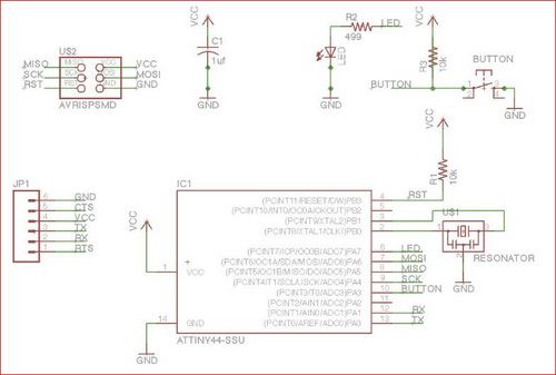
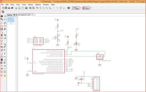
Designing the circuit in Eagle CAD.
The components used were downloaded from fab.lbr and listed below
1
ATTINY44A-SSU
2
20 MHz Resonator
3
AVRISP 2X3 Header
4
FTDI
5
LED
6
1K Resistor
7
10K Resistor
8
1 microfarad capacitor
9
button
Downloaded fablab.lbr and put it into C:\EAGLE-7.5.0\lbr - (This is the folder of my choice to save my Eagle CAD, you can do so your own)
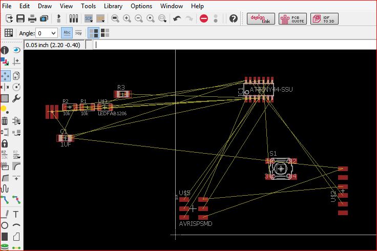
Now launch the Eagle CAD and click on File, New and Schematic. Placed all the components in the schematic work space and label them accordingly.
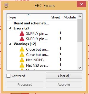
One important thing to note is the Electrical Rule Check - ERC which is used only in Schematic Window.
Click on Tools and ERC to run checks.
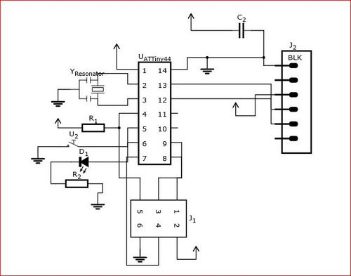
The purpose is to check whether there were any open connections or nil values assigned to the connectors. If there were errors, it will be displayed in the small window box as shown below. Hello-World Schematic
To see where the errors lays, just hover over it to read the error message and click on it to show the error on the schematic itself.
Hello-World Schematic
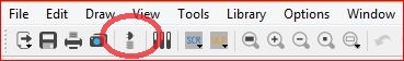
After that, click on the Generate/Switch to switch view between Board or Schematic page.
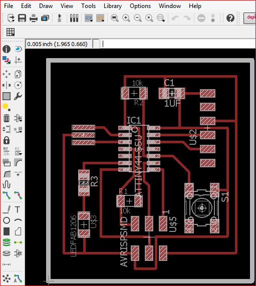
The laying out of the components onto the board. Hello-World Components Laying Out
The final layout of the components. Hello-World Final Laying Out
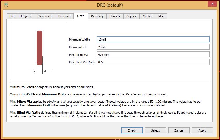
Another important thing to note is the Design Rule Check - DRC which is used only in Board Window.
Click on Tools and DRC to run checks.
We are only interested in the Clearance and Sizes at this point in time.
The purpose of Clearance Tab was to ensure the clearance between 2 signal paths do not go below the minimum clearance determined in the parameters box. Clearance
The purpose of the Size Tab is to ensure the width of the signal path is not below the minimum value determined in the parameters box. Sizes
It will determined the width and clearance of the signal paths when doing the Autoroute on the PCB board design.
Once all necessary adjustments were completed, save the files xxx.brd and xxx.sch into a flash drive.
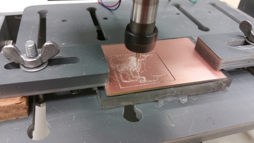
PCB Milling
Launch the EagleCAD in the computer that has the CNC USB Controller application in it. Because the PCB-GCODE application builted into CNC USB Controller is a paid licence application. Afterwhich open up the xxx.brd and xxx.sch files in that computer that has EagleCAD installed.
These are the steps that must be followed up.
1) Click File and Run ULP in the Board environment.
2) Click on folder named pcb-gcode
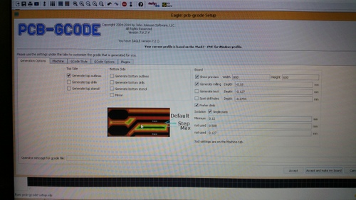
3) Click on pcb-gcode-setup.ulp and PCB-GCODE will launch
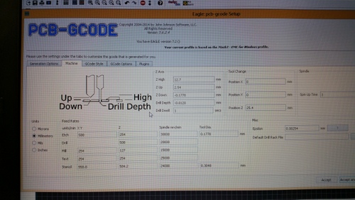
4) In the PCB-GCODE page, click on "Machine" tab and change the units from inches to millimeters
5) Go back to "Generation Options" tab
6) On the "Top Side" tab, check only "Generate Top Outlines"
7) On the "Bottom Side" tab, uncheck all
8) On the "Board" tab, check on
(i) Show Preview
(ii) Generate milling; Depth = 0.1
(iii) Prefer Climb
(iv) Single Pass; minimum = 0.1
9) Click on "Accept and Make My Board"
10) View and check on sketches, especially the lines on the path and pads
11) Click OK to close and exit all related windows
12) Go back to the location where the xxx.brd and xxx.sch were kept in the first place
13) Look for xxx.top.etch.tap
14) Go back to CNC USB Controller and click File, Open to look for this file mentioned above
15) Click Open
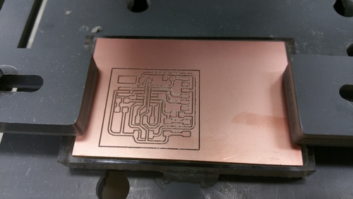
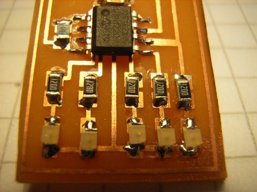
Applied a thin cat of solder onto all the pads where the components will sit. This will allow a easier time when soldering components onto the PCB. Hello World board completed
My comments
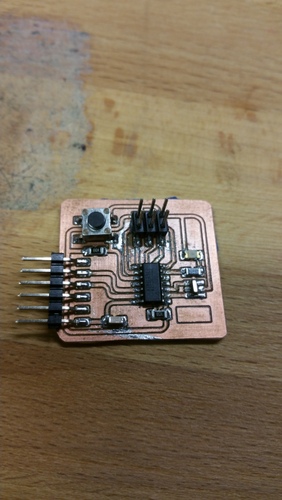
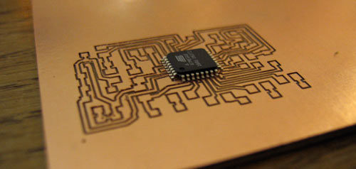
The only thing I find most useful is the eagle cad. You can named and placed the components in the schematic without actually the need to connect them. Quite interesting. The making of this echo hello world board is most frustrating. I felt the SMD is unsuitable for this type electronic built . The components were too small, difficult to read its value, easily spring off and permanently displaced. The soldering process is a especially painful because the solder kept shorting across it's pad to adjacent copper path. This type of soldering proces are usually and should be done by machine and error free and patience test free. Another area that can reduce the frustration is to remove the copper completely that aren't used. Copper Removal Method
Instead of just scratching through a thin route for connectivity pathway
Isolation Milling Method
This will certainly reduce the chances of solder shorting across two different paths. I wondered why we can't do it like as in the first picture shown
 to switch view between Board or Schematic page.